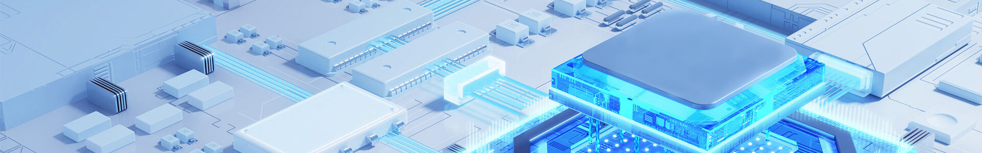
The field of printed circuit board (PCB) design is rapidly evolving, encompassing everything from layout intricacies to the final production stage. As technology advances, so do the methods used in PCB design, with innovations like the introduction of multi-layer boards and the incorporation of various modern materials. This evolution emphasizes the crucial role of PCB assembly services and the need to stay updated with these cutting-edge trends. A notable shift includes the integration of automation in PCB design processes, which significantly enhances efficiency and reduces the likelihood of errors. Furthermore, using advanced PCB manufacturing techniques allows for more compact and reliable products.
Keeping abreast of PCB design trends is vital for companies seeking to maintain or grow their market share. Those unwilling to adapt may experience a decline in their competitive standing. Indeed, research and industry analyses, such as those from IPC, underscore the importance of integrating modern design techniques to remain relevant. Incorporating innovative approaches and technologies ensures that companies can keep pace with the rigorous demands of the electronics market, providing a strategic advantage in both production capabilities and long-term sustainability.
Technological advancements are profoundly reshaping PCB design, particularly with the rise of IoT devices and high-frequency applications. The Internet of Things (IoT) demands PCBs that can accommodate diverse and complex functionalities while maintaining reliability and performance. The integration of cutting-edge technologies such as AI and machine learning into PCB assembly further enhances the precision and efficiency of PCB manufacturing and assembly, facilitating the production of boards that meet the rigorous demands of modern electronics. Additionally, advancements like high-frequency PCBs are crucial for new-age communication technologies including 5G, enabling unprecedented data transfer rates and connectivity.
The growing market demand for compact and efficient PCB designs mirrors the broader trend towards miniaturized electronics. As consumer electronics increase in sophistication and decrease in size, the necessity for intricate and space-saving PCBs becomes evident. This shift has fueled the demand for high-density interconnect (HDI) boards that accommodate more components within smaller areas, ensuring robust performance despite limited space. PCB designers are continually innovating to compress functionality into reduced footprints, a necessity driven by the proliferation of devices like smartphones, tablets, and smartwatches. This trend is closely tied to enhanced PCB design techniques and the consistent push for miniaturization, reinforcing the vital role of pcb circuit board manufacturers in developing increasingly compact and efficient PCBs.
The trend towards miniaturization and high-density interconnects (HDI) is becoming increasingly crucial in printed circuit board design. Today's electronic devices, especially wearables and mobile technology, demand more functionality in limited spaces. The integration of more components within these compact areas enables enhanced features and improved performance, meeting the growing needs of industries like wearable technology and communications.
Flexible and rigid-flex PCBs are revolutionizing design versatility across various sectors. Such designs are prevalent in automotive electronics and medical devices, supporting the development of products that require flexibility and resilience. These PCBs allow circuit designers to overcome constraints associated with traditional rigid boards, promoting innovative and adaptable solutions tailored to unique specifications.
Sustainability and eco-friendly practices in PCB manufacturing are also gaining traction. Manufacturers are increasingly adopting green materials and eco-conscious production processes to minimize environmental impact. This shift is in response to global trends and regulatory requirements aimed at reducing carbon footprints and electronic waste. PCB manufacturers are exploring biodegradable materials and recycling strategies, which align with environmental goals and elevate the industry's sustainability standards.
Advanced technologies are reshaping the landscape of printed circuit board (PCB) design by introducing efficient and innovative methodologies. Implementations of Artificial Intelligence (AI) and Machine Learning (ML) play a pivotal role in enhancing decision-making and streamlining design processes. This advanced approach significantly reduces time to market, which is seen as essential by experts in the electronics field. By automating tasks and predicting outcomes, AI and ML provide designers with the tools needed to optimize performance and ensure the reliability of PCB designs.
Moreover, additive manufacturing and 3D printing are revolutionizing PCB design by enabling rapid prototyping and reducing waste. This method offers manufacturers flexibility in creating complex designs that would be otherwise constrained by traditional manufacturing techniques. By facilitating a more adaptive development phase, these technologies allow designers to iterate and innovate quickly, ensuring that new products meet rigorous standards and performance expectations. As they become more integrated into the design and manufacturing processes, these technologies are proving invaluable, especially during product development phases, creating a future where PCB circuit board manufacturers can quickly adapt to changes in consumer needs.
Adapting to new technologies presents multiple challenges for PCB circuit board manufacturers. One primary challenge is the necessity for ongoing employee training to keep up with evolving technological advancements in the industry. Additionally, investing in modern equipment can be a significant financial burden, particularly for smaller manufacturers who struggle to compete with larger firms. These costs can act as a barrier, hindering the ability of smaller PCB makers to adopt innovative technologies as quickly as larger players in the market.
However, embracing these new technologies also opens up substantial opportunities for growth and innovation. Manufacturers that successfully adapt can differentiate themselves through enhanced product offerings and improved operational efficiencies. By improving their capabilities, these companies can gain a competitive edge in the PCB manufacturing sector. This advancement not only boosts their product quality but also enhances their overall market position, helping them to stand out amid a crowded and fast-evolving industry landscape. Ultimately, the ability to incorporate cutting-edge technologies in their processes results in more robust, reliable, and advanced PCB solutions, aligning with the increased demand from fields such as AI and IoT that rely heavily on sophisticated PCB designs.
Quality PCB assembly services are vital for the reliability and performance of electronic devices. Without proficient assembly, electronic components can fail, leading to costly financial losses and damaging reputations. This underscores the necessity for high standards and precision in the assembly process.
Collaborating closely with PCB manufacturers enhances the understanding of specifications and lead times. In today's fast-paced technology landscape, this collaboration is crucial as it directly impacts production efficiency and delivery schedules. Such partnerships are essential to keep pace with the demands of innovation and market competition.